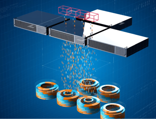
We have numerous partners and alliances in the Solid State drive (SSD) space that we interact with regularly. Conversations in related meetings with those allies continues to revolve around the same issue, overcoming performance bottle necks at the storage level. In attacking this problem to get higher performance for things like boot times, application load times, etc., the industry has turned to flash memory, otherwise referred to SSDs (we'll also be announcing a brand new SSD technology in the next few weeks).
The following may be well known to those highly knowlegdable in SSDs, but hopefully helps others less versed in their design.
High end SSDs have proven to yield some very impressive read times, well over double a typical SATA hard disk drive in some cases.
Here are some example published speeds from a few manufacturers/models:
Seagate 7200.12 HDD 500GB, 750GB, and 1TB family
Read/Write speeds (outer tracks, empty drive): 125MB/sec sustained, 160MB/sec peak
Intel X25-M 80GB SSD (MLC)
Sequential Access – Read: up to 250MB/s
Sequential Access – Write: up to 70MB/s
Intel X25-M 120GB SSD (MLC)
Sequential Access – Read: up to 250MB/s
Sequential Access – Write: up to 100MB/s
Intel X25-E 32GB SSD (SLC)
Sequential Access – Read: up to 250 MB/s
Sequential Access – Write: up to 170 MB/s
One of the main reasons for such fast read times is the lack of “seek time” that an SSD has to find and retrieve a piece of data versus a hard drive. Simply put, a hard drive has to move a magnetic head connected to an arm over a track on a platter and then through various means find the data requested and read or write something.

Now you have to admit, a hard drive does this quite well and very fast, considering the physics involved.
On the other hand an SSD sends an electrical pulse to read the data which is much faster in comparison; give or take on the order of magnitude, double on higher end SSDs. The lack of a moving part cuts the time down considerably.
Now, writing data to SSDs is a whole other story which leads us down a bit of a rabbit hole so to speak and the main subject of this blog.
SSD DNA
To start with, let’s look at what an SSD is:
Note, I have borrowed some photos and descriptions from the following site: www.popsci.com/category/tags/ssd.
Firstly you simply have a small piece of silicon with a whole lot of transistors that look like the following:

Each transistor is 1000 times thinner than a human hair. In essence, each transistor either holds an electrical charge or it doesn’t. In the case of SSDs, a transistor that is charged equals the value 0 and the ones that are not equal a value of 1. That is the extent of it.
In the above photo the transistor that is charged has a circle around the “e” which stands for electrons representing the charge.
Now, to read what’s inside these transistors an electrical pulse is sent to them and by reading the signal from the pulse sent it’s able to tell which are charged and which are not. All in all this is a pretty fast operation. Even writing to a transistor for the first time is pretty fast as it’s empty with no charge to begin with.
BUT…… what happens when you have to write to an area of the SSD that has already been written to? Here in lays the problem and the unfortunate “Achilles heel” for SSDs. With a hard drive you can just simply flip the bit in place and call it a day. In fact this is a faster operation on a hard drive then it is on an SSD, over the long run. Now aside from the extra step it takes to erase an SSD it gets a lot worse. But in order to understand this we need to view how data is laid out on an SSD:
The smallest unit is a single transistor, also known as a cell. Imagine the dot shown is a top view of a single transistor magnified a gazillion times.

This single transister holds a single bit of data, i.e. a 1 or a 0. The next unit size up is a called a page and holds 4KB of data. To put this in perspective, there are 8,192 bits in one kilobyte so each page contains 32,768 transistors. A page is the smallest unit that can be written to on the SSD. This means that even if the data you are writing is only 1,500 bits in size, it will use up the entire 4KB of space and make it unusable for writing other data. You only get to write once to it until its been erased for reuse again.

In fact, to update the data within this page, the data would have to be copied first, updated and rewritten to a new page leaving the old page unusable till it’s been erased. The controller has to earmark it for clean up so it can be used again later.
Now, even though this page has been earmarked for being erased, it may not get erased for some time because it’s actually part of a bigger group of data called a “block”. A block is a group of pages as illustrated below:

The number of pages that make up a block may vary from one SSD model to another and can be very large (in the megabytes). On one such SSD we have tested on, this happens to be 128k, which would be a group 32 pages. This data block (32 pages) is actually what’s called an “erase block”. An SSD only erases one data “block” at a time. So back to our example of this page with old data in it: theoretically this page could sit around a while before this block of data is erased by the SSD. It’s plausible this could have in some cases security of data issues but that’s a subject for research and test.
Now, when data is updated in a page as discussed earlier it has to be moved to another location unbeknownst to the file system and internally mapped by the controller on the device to keep track of it as illustrated below:

There is obviously overhead associated with this. So a page, for argument sake, could have three states of existence:
Ready to be used (it’s erased or been erased thus all transistors have been set to 1) as in the clear little boxes above;
Used — as in the blue boxes above;
Dirty (containing invalid data that needs to be erased) as in the black boxes above.
The overhead in handling dirty data is huge, and referred to as garbage collection. Garbage collection is the process of moving good data out of areas where old data exists in order to erase the old data in order to reclaim pages that can be written to again.
Doing a lot of this garbage collection activity creates a lot of activity called “write amplification”.
This is the disease that SSDs are plagued with which kills their write performance, particularly as the device fills up. It’s also what shortens the life span of the device.
The following is a definition or description from Wikipedia that I think is pretty good:
“Write amplification (WA) is a phenomenon associated with Flash memory and solid-state drives (SSDs). Because Flash memory must be erased before it can be rewritten, the process to perform these operations results in moving (or rewriting) user data and metadata more than once. This multiplying effect increases the number of writes required over the life of the SSD which shortens the time it can reliably operate. The increased writes also consume bandwidth to the Flash memory which mainly reduces random write performance to the SSD. Many factors will affect the write amplification of an SSD, some can be controlled by the user and some are a direct result of the data written to and usage of the SSD.”
Now, there is a comment that is made in the above description that is interesting, and could lead to read performance in some cases getting degraded, which is the “increased writes” consuming bandwidth to the Flash memory interrupting a read operation.
Now, I don’t say this as a fact but rather postulating whether or not reads are affected.
The overhead in writes required by the Windows NTFS file system to do just one IO could be considered extreme from the SSD’s point of view. To create and write one bit of information, such as a notepad doc with a single number in it, requires an update to the MFT file by creating a record of the operation, update to a directory file and any other metadata files such as journal files that are keeping track of operations at the time. The point is, for every one write of user data there are several writes occurring to keep track of it.
Current file systems were designed based on hard disk drive characteristics, not SSDs. From the SSD’s point a view, NTFS writes with wild abandon. This puts a lot of overhead on the SSD controllers with a lot of overhead on data mapping and housekeeping at the controller level of the SSD which hard drives don’t have to worry about much. A hard drive typically only has to re-map data when it has a bad sector on it as an example.
NTFS file system thinks for example that a file should be split in two (split IOs) because it thinks it doesn’t have a contiguous free space for the file that is being updated. Yet the SSD may have, during its garbage collection process created a space or remapped data clusters but the operating system doesn’t know this and vice versa.
The current TRIM functionality is supposed to help SSDs within Windows 7 but it's far from being a panacea to the write amplification issue.
Different types of SSD
SLC stands for “single level cell”
MLC stands for “multi level cell”
TLC stands for “tender loving care". okay not really, just checking to make sure you are paying attention. It really stands for" tri level cell”; really.
SLC is faster than MLC and TLC.
The design of an MLC and an SLC are pretty much the same. The difference is an MLC is able to put more than one value in a single transistor (referred to as a cell) by layering the data within the cell. Typically two or more bits are able to be placed in a single cell with MLC versus one bit in SLC.
So MLC is able to contain twice as much data versus SLC. That’s the plus side. The down side is MLC in reading and writing data to a single cell has to be very precise and has a lot of overhead logic wise, so MLC ends up slower than SLC due to the preciseness that is required to determine if two values exist and what those values are in a single cell. Also the life cycle of MLC becomes 10x shorter than SLC. The following is a great white paper that describes the differences very well and how voltages are used to read the values, etc. https://www.supertalent.com/datasheets/SLC_vs_MLC%20whitepaper.pdf
The difference between TLC and MLC is NOT more transistors. L stands for "level", referring to voltage level to a transistor, not multiple levels or numbers of transistors. Again the above link along with a few other sites lays this out fairly well.
The difference between one flash memory or SSD is not so much the chip itself but the supporting controller and its design. This includes creating multiple data channels, on-board Raid and other fancy and expensive solutions. The other differentiator is software within the controller managing all of the mapping of data, moving data around, etc. Sounds like the age-old fragmentation problem to me again; just at a slightly different level.


Leave A Comment
You must be logged in to post a comment.